PCB manufacturing & Protyping

At ATEK Engineering Solutions LLP, we provide precision PCB manufacturing solutions designed for reliability, performance and long-term serviceability. From PCB layout and fabrication to inspection and finishing, we combine engineering expertise with controlled manufacturing processes to deliver PCBs for industrial, defence, automotive, instrumentation and other demanding applications.

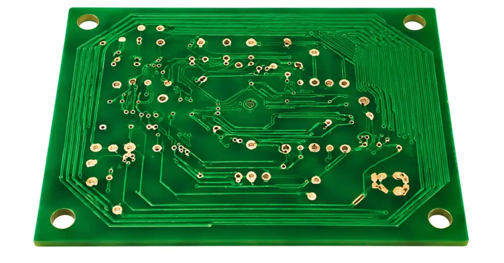
Single Layer PCB

Single-layer PCBs offer a cost-effective solution for simpler electronic circuits, with conductive tracks on one side of the board. They are widely used in power supplies, control circuits, instrumentation and general electronics.

PCB Specifications Table

01

Minimum Conductor Width

6 mils (0.15 mm)
02

Minimum Conductor Spacing / Air Gap

6 mils (0.15 mm)
03

Minimum Plated Hole Size

16 mils (0.4 mm)
04

Maximum Plated Hole Size

240 mils (6 mm)
05

Maximum Board Size

250 mm × 350 mm
06

Maximum Number of Layers

10
07

Minimum Copper Thickness

1 Oz (35 microns)
08

Maximum Copper Thickness

3 Oz (105 microns)
09

Dedicated Electrical Testing (BBT)

Available
10

PCB Cutting Options

Routing, V Groove

Product Finish

01

Single Sided

HAL, Lacquer
02

Double Sided

HAL, Electroplated Gold & Nickel
03

Solder Mask Finish

PISM
04

Solder Mask Color

Green, White, Black, Blue, Red
05

Legend / Ident Color

White, Black, Yellow, Green

Product Raw Material

01

PCB Base Material

FR1, FR4, CEM1, CEM3, Metal Clad
02

Board Thickness (in mm)

0.8 to 3.2 mm

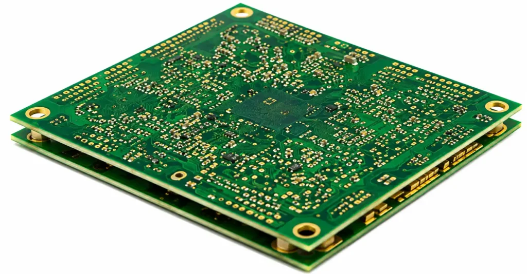
Double Layer PCB

Double-layer PCBs have conductive copper layers on both sides, interconnected through plated-through holes and vias. They provide greater circuit density and routing flexibility while remaining economical for a wide range of applications.

Benefits of Double Sided PCBs

  • More Flexible to Design
  • Increased Circuit Compactness
  • Relatively Cost-Effective
  • Transitional Level of Circuit Density
  • Compact Board Size (which can reduce costs)
  • PCB Specifications Table

    01

    Minimum Conductor Width

    6 mils (0.15 mm)

    02

    Minimum Conductor Spacing / Air Gap

    6 mils (0.15 mm)

    03

    Minimum Plated Hole Size

    16 mils (0.4 mm)

    04

    Maximum Plated Hole Size

    240 mils (6 mm)

    05

    Maximum Board Size

    300 mm × 350 mm

    06

    Maximum Number of Layers

    2

    07

    Minimum Copper Thickness

    1 Oz (35 microns)

    08

    Maximum Copper Thickness

    3 Oz (105 microns)

    09

    Dedicated Electrical Testing (BBT)

    Available

    10

    PCB Cutting Options

    Routing, V-groove, Punching

    PCB Surface Finish and Masking Specifications

    01

    Single Sided

    HAL, Lacquer

    02

    Double Sided

    HAL, TIN, Electroplated Gold & Nickel

    03

    Solder Mask Finish

    PISM, Liquid Solder Mask

    04

    Solder Mask Color

    Green, White, Black, Blue, Red

    05

    Legend / Ident Color

    White, Black, Yellow, Green

    06

    Special Requirement

    Carbon Printing on Push Button, Selective Gold & Nickel Plating on Connecting Tabs

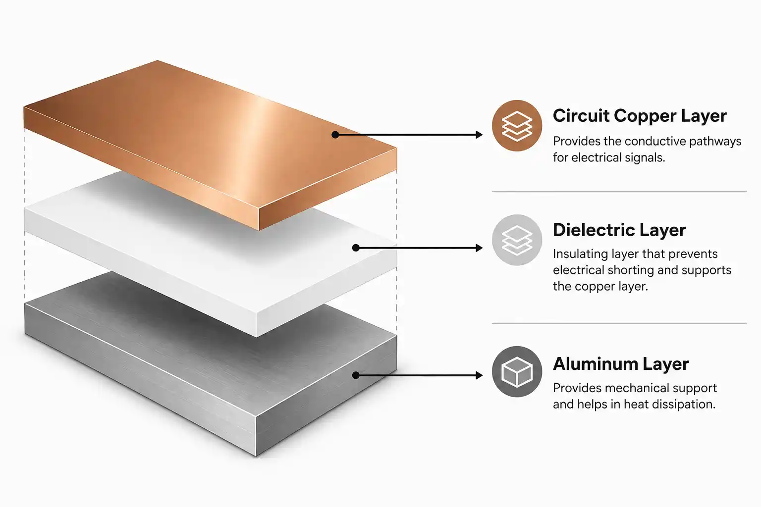
    PCB Metal
    PCB Metal

    01

    Minimum Conductor Width

    6 mils (0.15 mm)

    02

    Minimum Conductor Spacing / Air Gap

    6 mils (0.15 mm)

    03

    Minimum Plated Hole Size

    16 mils (0.4 mm)

    04

    Maximum Plated Hole Size

    240 mils (6 mm)

    05

    Maximum Board Size

    300 mm × 350 mm

    06

    Maximum Number of Layers

    2

    07

    Minimum Copper Thickness

    1 Oz (35 microns)

    08

    Maximum Copper Thickness

    3 Oz (105 microns)

    09

    Dedicated Electrical Testing (BBT)

    Available

    10

    PCB Cutting Options

    Routing, V-groove, Punching
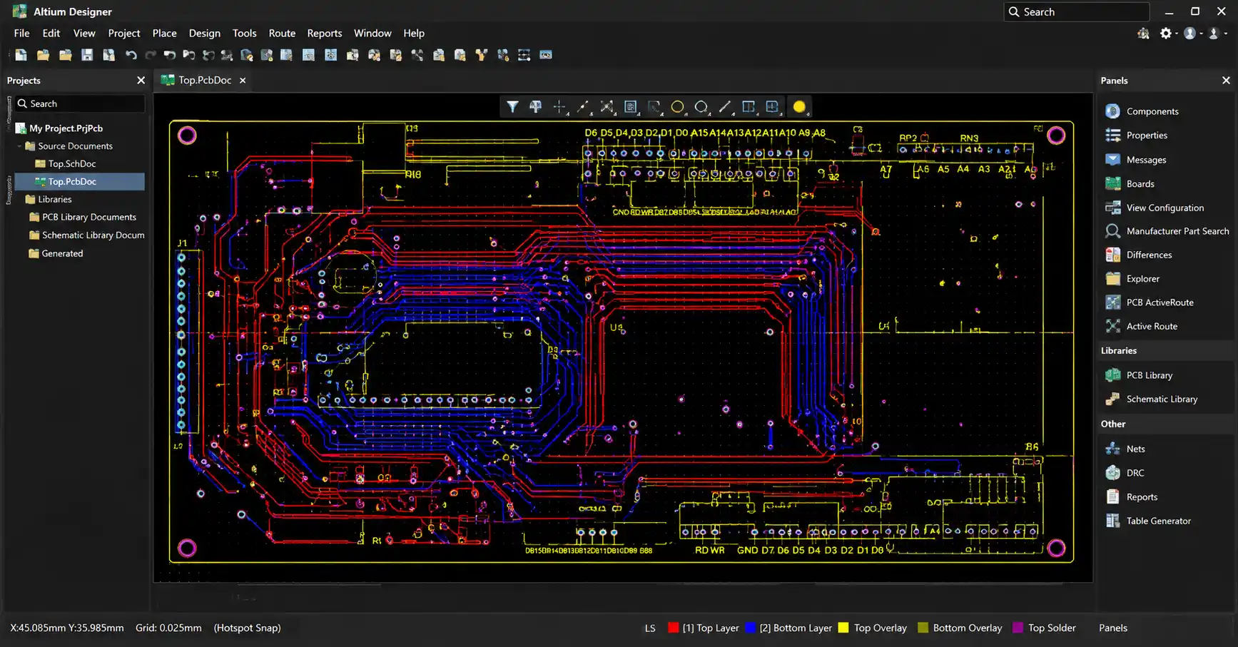
    PCB Layout & Design

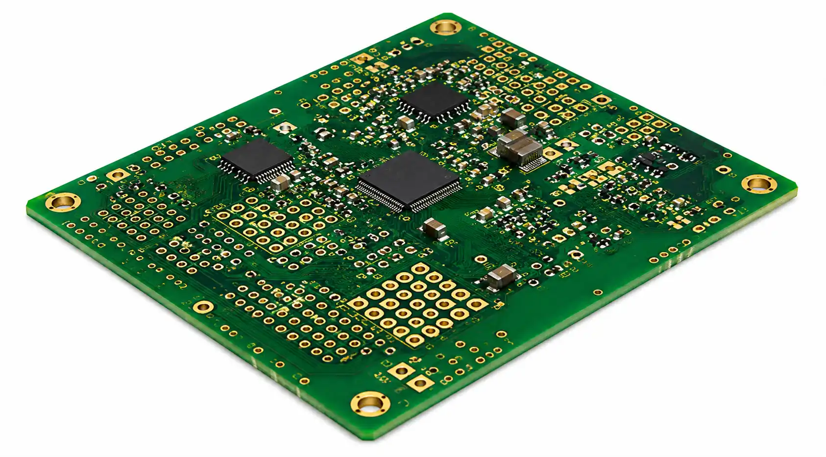
    Our PCB layout services convert circuit schematics into manufacturable, reliable and optimized PCB designs. We focus on component placement, signal integrity, power distribution, thermal considerations, EMI/EMC requirements, manufacturability and serviceability.
    • Single, Double and Multi-layer PCB Designs
    • High-speed PCB Layouts for complex applications
    • Rigid, Flex and Rigid-Flex PCB Layouts
    • Analog, Digital and Mixed-Signal Board Designs
    • Impedance Control and Signal Integrity Optimization
    • Thermal Management and Power Distribution Solutions
    • Design for Manufacturability (DFM) and Design for Testability (DFT)

    Why Choose MRK Electronics?
  • Experienced Design Engineers: Our team has hands-on experience across various industries including automotive, industrial, consumer electronics and healthcare.
  • Latest Tools and Technologies: We use industry-leading software like Altium Designer, OrCAD, Eagle and more.
  • Customized Solutions: Every design is tailored to your project’s unique specifications and production needs.
  • Fast Turnaround Time: We understand project deadlines and ensure your design moves to production faster.
  • Quality Assurance: Each layout undergoes a strict review and validation process to guarantee performance and reliability.
  • PCB Fabrication – Rigid

    We manufacture rigid PCBs to meet application-specific electrical, mechanical and environmental requirements. Our capabilities include precision drilling, imaging, etching, plating, solder mask, surface finishing and inspection, supporting prototype as well as production requirements.

    Our Rigid PCB Fabrication Capabilities:

    • Single, Double and Multi-layer Rigid PCBs (up to 24+ layers)
    • High-Density Interconnect (HDI) Boards
    • FR4, High-TG and Special Material Options (Rogers, Polyimide, etc.)
    • Surface Finishes: HASL, ENIG, Immersion Silver, OSP and more
    • Fine Line and Microvia Technology
    • Controlled Impedance and High-frequency PCB Fabrication
    • Lead-Free and RoHS-compliant Fabrication

    Why Choose MRK Electronics?
  • Advanced Manufacturing Facilities: Equipped with the latest fabrication technologies.
  • Strict Quality Control: Each board undergoes rigorous testing — including AOI (Automated Optical Inspection), X-ray inspection and electrical testing.
  • Fast Turnaround and On-Time Delivery: From prototype to mass production, we ensure timely delivery without compromising quality.
  • Cost-Effective Solutions: Competitive pricing with no hidden charges.
  • Customization: Full flexibility in board thickness, copper weight, solder mask color and more.
  • PCB Fabrication – Flexible

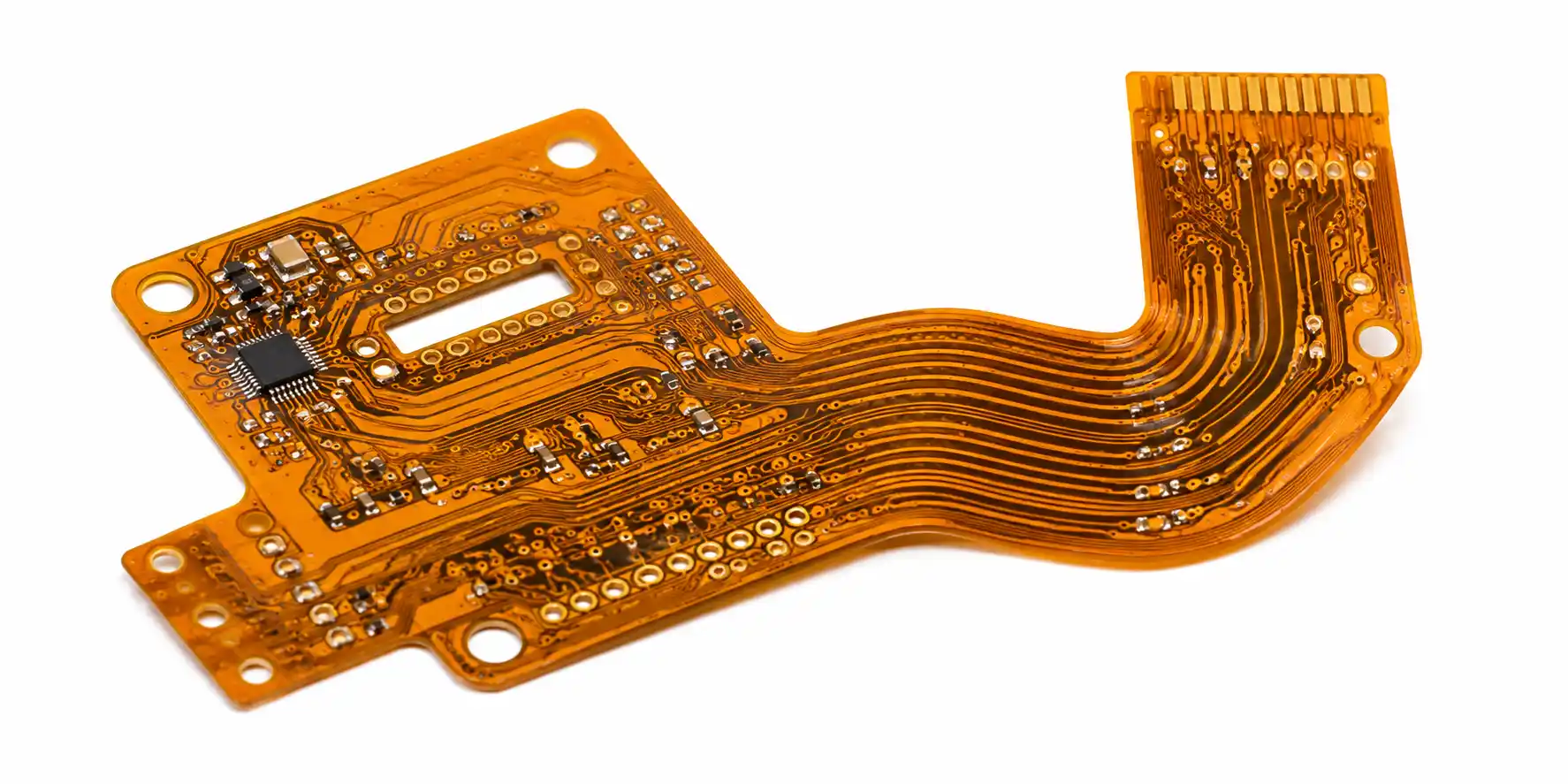
    Flexible PCBs provide lightweight, space-saving interconnections where conventional rigid boards are unsuitable. They are ideal for applications requiring bending, folding, compact packaging or dynamic movement, including instrumentation, automotive, aerospace and defence electronics.

    Our PCB Fabrication Capabilities:

    • Single, Double-Sided and Multi-layer Flex PCBs
    • High-Density and Fine-Pitch Flex Circuits
    • Advanced Materials: Polyimide, PET and other flexible substrates
    • Surface Finishes: ENIG, Immersion Tin, OSP and more
    • Stiffener Integration (PI, FR4, Stainless Steel)
    • Dynamic Flexibility and Bend Reliability
    • Controlled Impedance and EMI Shielding Options
    • RoHS and Lead-Free Compliant Fabrication

    Why Choose MRK Electronics?

    • High Precision Manufacturing: Tight tolerances and superior craftsmanship.
    • Customization: Tailored designs for specific space-saving and mechanical requirements.
    • Reliability: Durable under repeated flexing, vibration and dynamic stress.
    • Fast Prototyping to Production: Speedy delivery from concept to final product.
    • Comprehensive Quality Assurance: 100% E-test, AOI inspection and IPC standards compliance.
    PCB Stensil

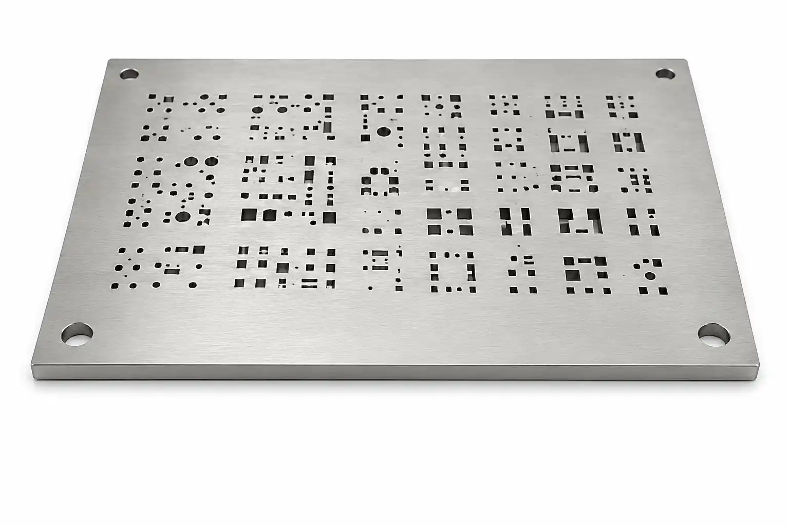
    We provide precision stainless-steel SMT stencils for accurate solder-paste deposition during PCB assembly. Stencils are manufactured to suit component geometries and assembly requirements, helping achieve consistent paste volume, placement accuracy and improved assembly yield.

    Our PCB Stencil Capabilities:

  • Laser-Cut Stencils: High-precision stencils for accurate solder paste application
  • Chemical Etched Stencils: Ideal for fine-pitch components and small apertures
  • Hydroformed Stencils: Best for very fine-pitch designs and complex geometries
  • Step-Stencils and Dual-Frame Stencils for versatile assembly processes
  • Micro-Measurement Stencils for ultra-fine components like BGAs (Ball Grid Arrays)
  • Customized Aperture Designs to optimize solder paste volume and consistency
  • Full Range of Stainless Steel and Nickel Plated Stencils
  • Why Choose ATEK Engineering Solutions?

  • Precision Engineering Advanced laser cutting and etching technology delivers highly accurate stencils with exceptional quality and consistency.
  • Enhanced Performance Achieve uniform solder paste application, minimize printing defects and improve overall solder joint reliability.
  • Rapid Turnaround Fast and efficient stencil fabrication to meet the demands of both prototype development and high-volume production.
  • Custom Solutions Stencils precisely engineered to match your PCB design, including customized apertures, dimensions and frame sizes.
  • Cost-Effective Solutions Competitive pricing with reliable quality, making our stencil solutions suitable for both small-batch and large-scale production.
  • PCB Manufacturing & Prototyping

    From initial design validation to production-ready boards, our PCB manufacturing and prototyping services help bring your electronic concepts to life with speed, precision and reliability. We support rapid prototyping, PCB fabrication, assembly, testing and design validation for a wide range of electronic applications.

    Our PCB Prototyping Services

    • Rapid PCB Prototyping – Quickly develop and validate PCB designs before moving to mass production.
    • Single & Multilayer PCBs – Manufacturing solutions for simple as well as complex multilayer circuit boards.
    • PCB Assembly – Accurate component placement, soldering and assembly for functional prototypes.
    • Design Validation – Verify electrical performance, functionality and manufacturability before production.
    • Prototype Testing – Comprehensive testing to identify design issues and ensure reliable operation.
    • Production-Ready Development – Seamlessly transition validated prototypes into scalable manufacturing.

    Connect With ATEK.