
PCB manufacturing & Protyping
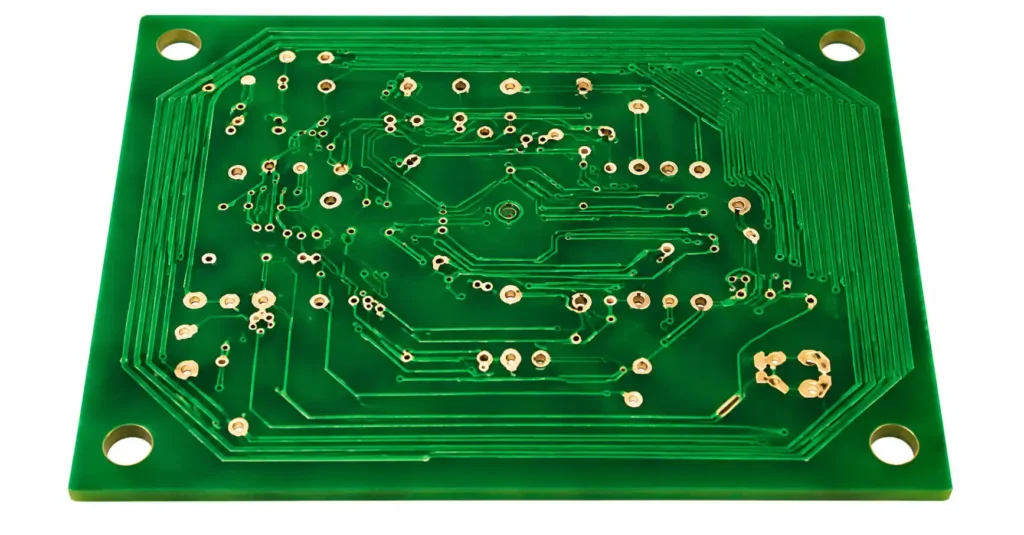
Single Layer PCB
PCB Specifications Table
Minimum Conductor Width
Minimum Conductor Spacing / Air Gap
Minimum Plated Hole Size
Maximum Plated Hole Size
Maximum Board Size
Maximum Number of Layers
Minimum Copper Thickness
Maximum Copper Thickness
Dedicated Electrical Testing (BBT)
PCB Cutting Options
Product Finish
Single Sided
Double Sided
Solder Mask Finish
Solder Mask Color
Legend / Ident Color
Product Raw Material
PCB Base Material
Board Thickness (in mm)
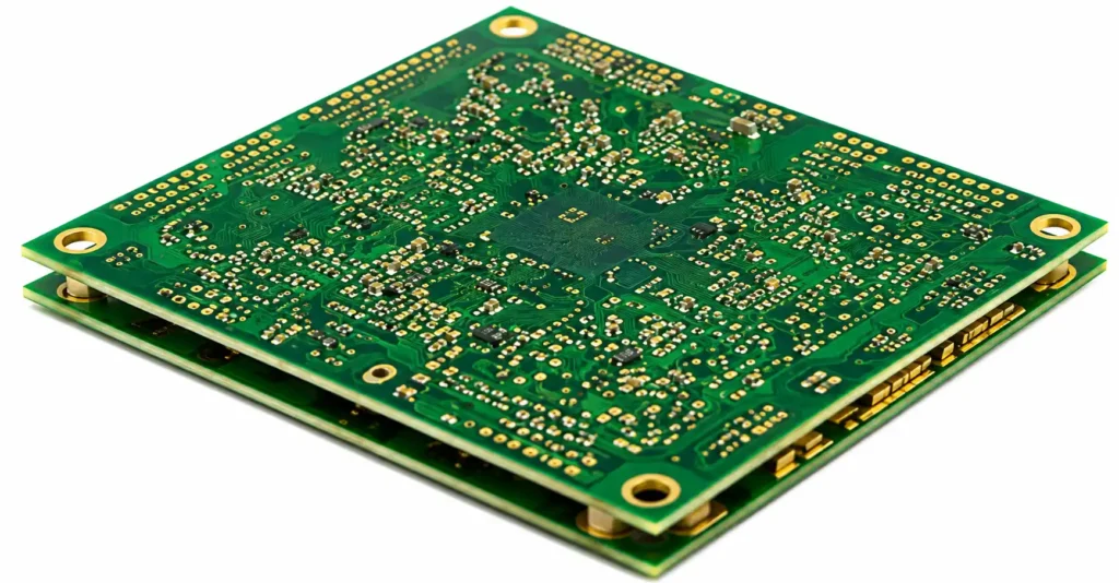
Double Layer PCB
Benefits of Double Sided PCBs
PCB Specifications Table
Minimum Conductor Width
6 mils (0.15 mm)
Minimum Conductor Spacing / Air Gap
6 mils (0.15 mm)
Minimum Plated Hole Size
16 mils (0.4 mm)
Maximum Plated Hole Size
240 mils (6 mm)
Maximum Board Size
300 mm × 350 mm
Maximum Number of Layers
2
Minimum Copper Thickness
1 Oz (35 microns)
Maximum Copper Thickness
3 Oz (105 microns)
Dedicated Electrical Testing (BBT)
Available
PCB Cutting Options
Routing, V-groove, Punching
PCB Surface Finish and Masking Specifications
Single Sided
HAL, Lacquer
Double Sided
HAL, TIN, Electroplated Gold & Nickel
Solder Mask Finish
PISM, Liquid Solder Mask
Solder Mask Color
Green, White, Black, Blue, Red
Legend / Ident Color
White, Black, Yellow, Green
Special Requirement
Carbon Printing on Push Button, Selective Gold & Nickel Plating on Connecting Tabs
PCB Metal
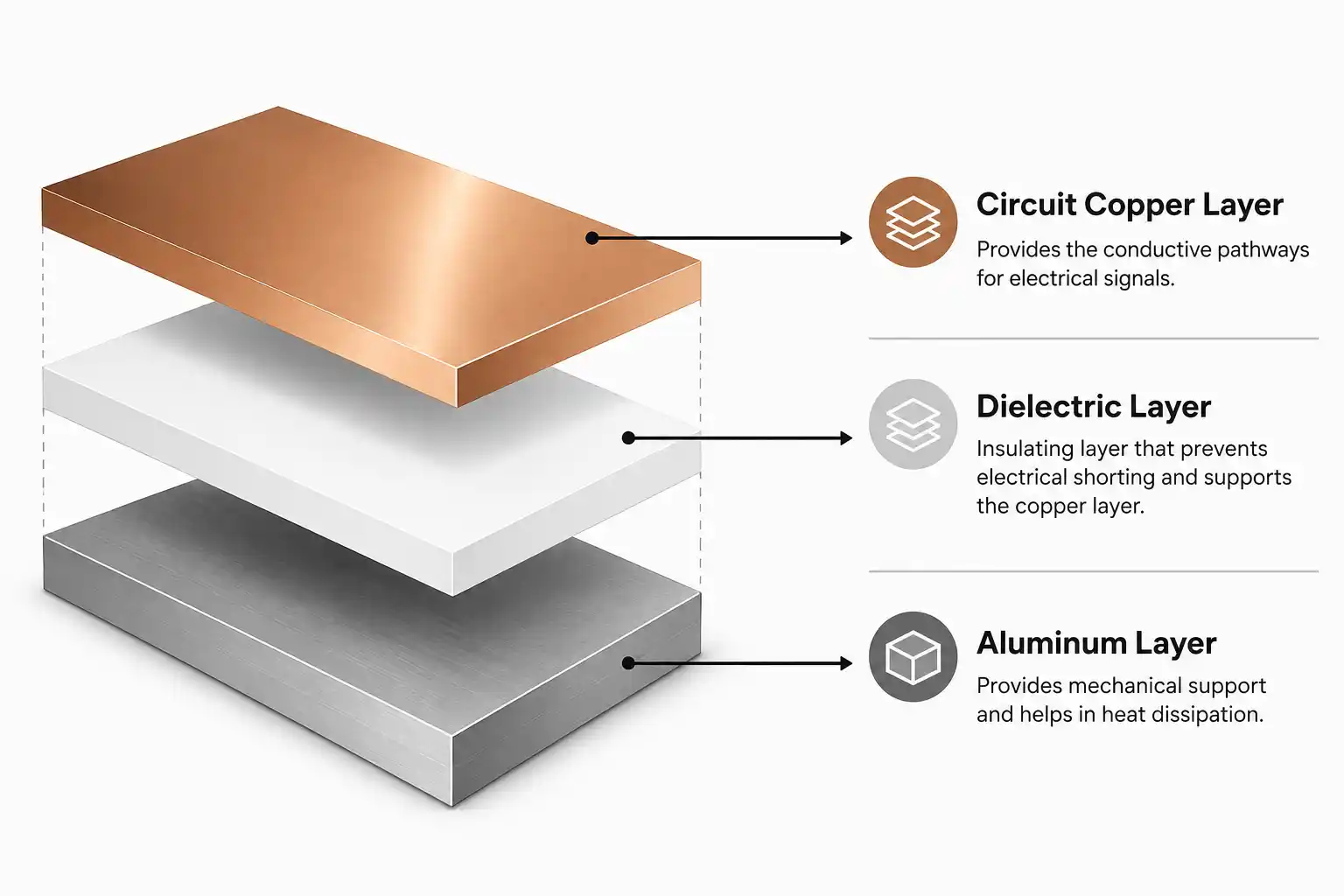
PCB Metal
Minimum Conductor Width
6 mils (0.15 mm)
Minimum Conductor Spacing / Air Gap
6 mils (0.15 mm)
Minimum Plated Hole Size
16 mils (0.4 mm)
Maximum Plated Hole Size
240 mils (6 mm)
Maximum Board Size
300 mm × 350 mm
Maximum Number of Layers
2
Minimum Copper Thickness
1 Oz (35 microns)
Maximum Copper Thickness
3 Oz (105 microns)
Dedicated Electrical Testing (BBT)
Available
PCB Cutting Options
Routing, V-groove, Punching
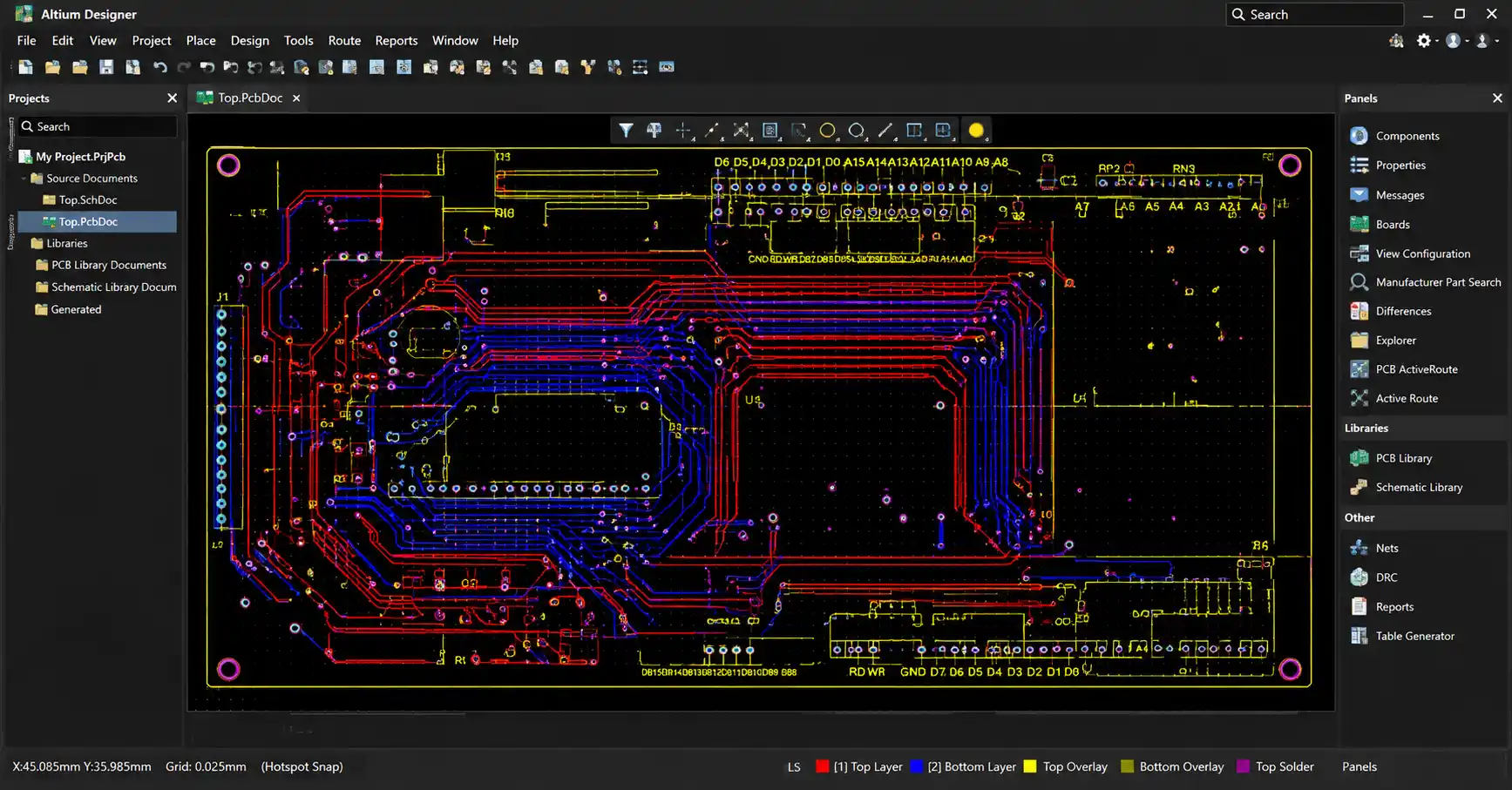
PCB Layout & Design
- Single, Double and Multi-layer PCB Designs
- High-speed PCB Layouts for complex applications
- Rigid, Flex and Rigid-Flex PCB Layouts
- Analog, Digital and Mixed-Signal Board Designs
- Impedance Control and Signal Integrity Optimization
- Thermal Management and Power Distribution Solutions
- Design for Manufacturability (DFM) and Design for Testability (DFT)
Why Choose MRK Electronics?
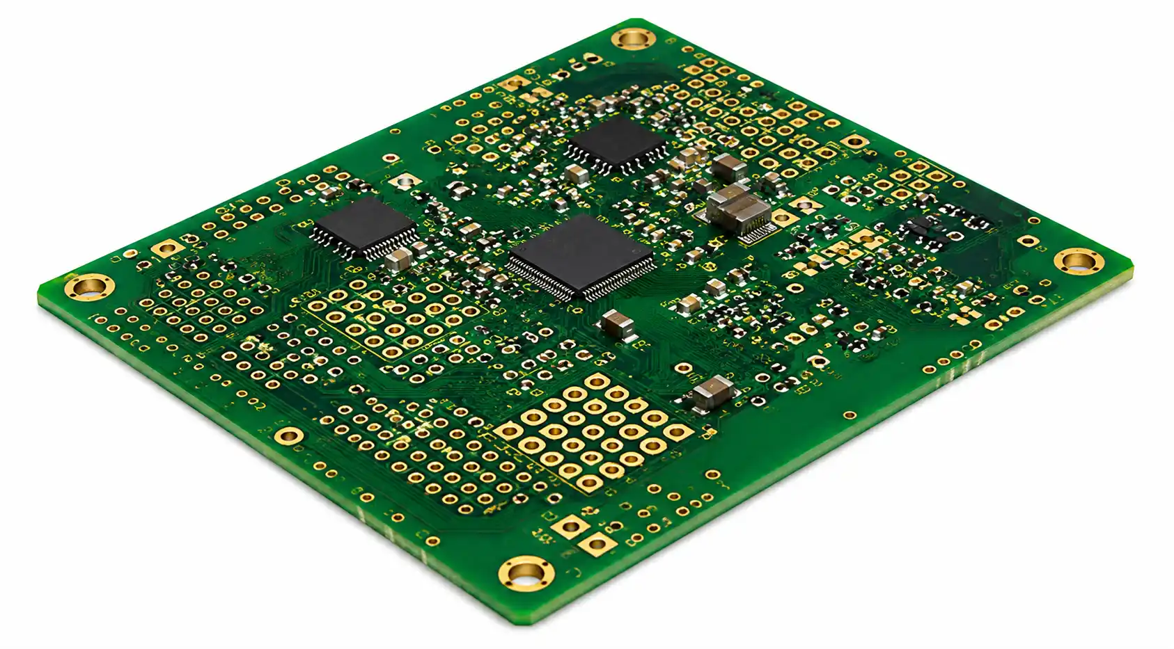
PCB Fabrication – Rigid
Our Rigid PCB Fabrication Capabilities:
- Single, Double and Multi-layer Rigid PCBs (up to 24+ layers)
- High-Density Interconnect (HDI) Boards
- FR4, High-TG and Special Material Options (Rogers, Polyimide, etc.)
- Surface Finishes: HASL, ENIG, Immersion Silver, OSP and more
- Fine Line and Microvia Technology
- Controlled Impedance and High-frequency PCB Fabrication
- Lead-Free and RoHS-compliant Fabrication
Why Choose MRK Electronics?
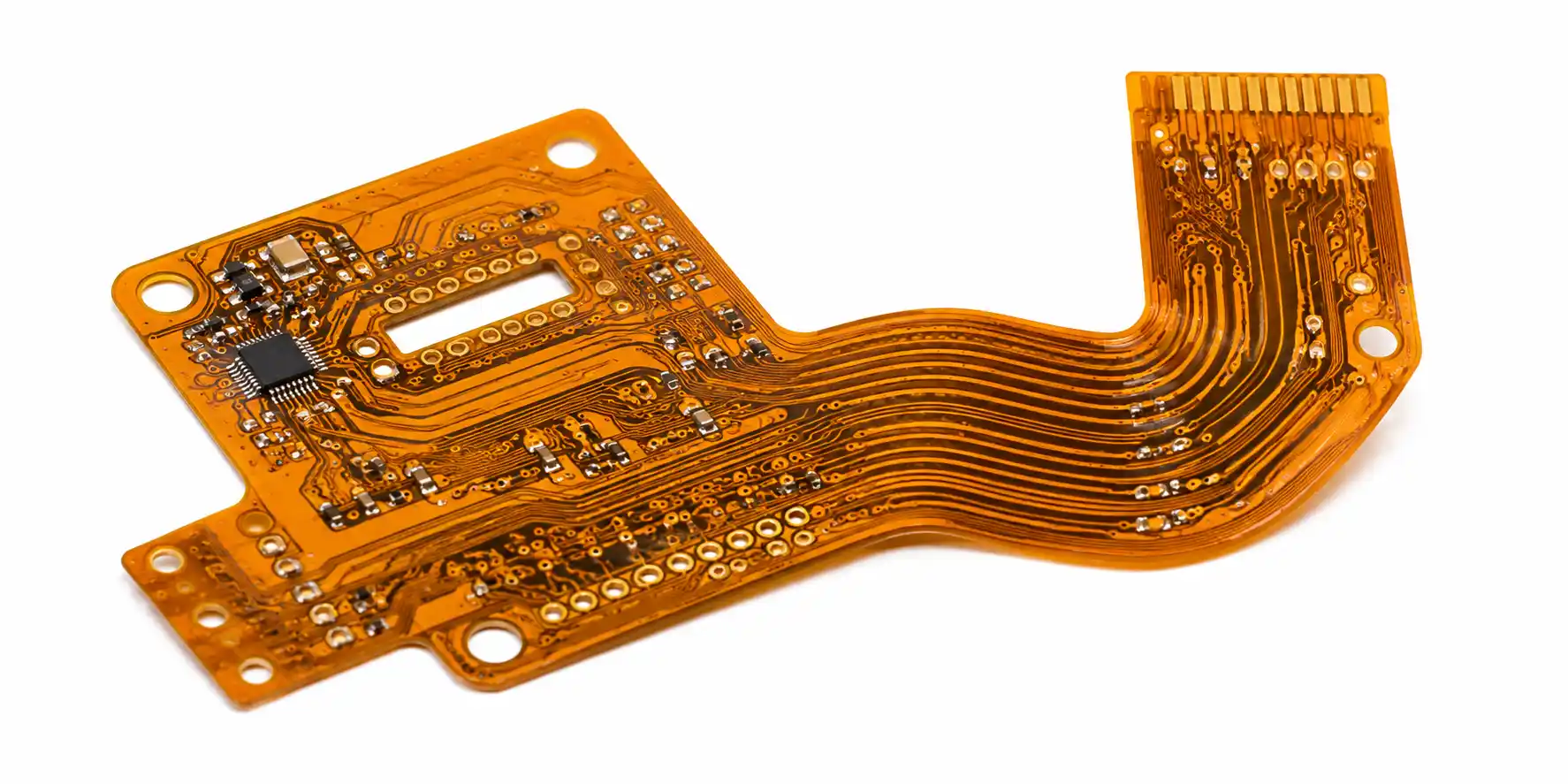
PCB Fabrication – Flexible
Our PCB Fabrication Capabilities:
- Single, Double-Sided and Multi-layer Flex PCBs
- High-Density and Fine-Pitch Flex Circuits
- Advanced Materials: Polyimide, PET and other flexible substrates
- Surface Finishes: ENIG, Immersion Tin, OSP and more
- Stiffener Integration (PI, FR4, Stainless Steel)
- Dynamic Flexibility and Bend Reliability
- Controlled Impedance and EMI Shielding Options
- RoHS and Lead-Free Compliant Fabrication
Why Choose MRK Electronics?
- High Precision Manufacturing: Tight tolerances and superior craftsmanship.
- Customization: Tailored designs for specific space-saving and mechanical requirements.
- Reliability: Durable under repeated flexing, vibration and dynamic stress.
- Fast Prototyping to Production: Speedy delivery from concept to final product.
- Comprehensive Quality Assurance: 100% E-test, AOI inspection and IPC standards compliance.
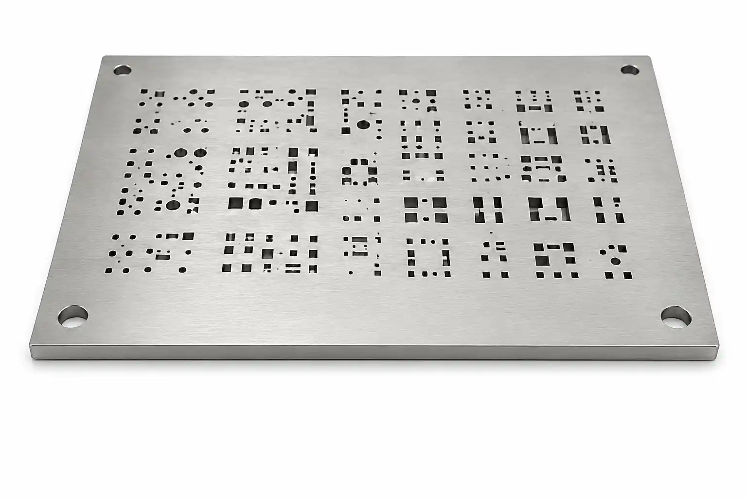
PCB Stensil
Our PCB Stencil Capabilities:
Why Choose ATEK Engineering Solutions?
PCB Manufacturing & Prototyping
From initial design validation to production-ready boards, our PCB manufacturing and prototyping services help bring your electronic concepts to life with speed, precision and reliability. We support rapid prototyping, PCB fabrication, assembly, testing and design validation for a wide range of electronic applications.
Our PCB Prototyping Services
- Rapid PCB Prototyping – Quickly develop and validate PCB designs before moving to mass production.
- Single & Multilayer PCBs – Manufacturing solutions for simple as well as complex multilayer circuit boards.
- PCB Assembly – Accurate component placement, soldering and assembly for functional prototypes.
- Design Validation – Verify electrical performance, functionality and manufacturability before production.
- Prototype Testing – Comprehensive testing to identify design issues and ensure reliable operation.
- Production-Ready Development – Seamlessly transition validated prototypes into scalable manufacturing.